|
Synopsys' New Silicon-Proven DesignWare USB 3.0 and USB 2.0 femtoPHY IP Cut Area by 50 Percent
5/7/2014 |
|
|
Small Footprint PHYs on 14/16-nm FinFET and 28-nm Processes Reduce Silicon Cost for Consumer, Mobile, Storage and Networking Applications
MOUNTAIN VIEW, Calif., April 29, 2014 /PRNewswire/ --
Highlights:
DesignWare USB 2.0 femtoPHY IP area is less than 0.2 sq. mm, and DesignWare USB 3.0 femtoPHY is less than 0.5 sq. mm, enabling designers to save PHY area and reduce overall silicon cost
DesignWare USB 3.0 femtoPHY includes full USB 2.0 support, enabling compatibility with billions of devices worldwide
Power down with data retention feature extends battery life while ensuring data preservation; support for USB Battery Charging v1.2 specification enables efficient charging of portable devices
The DesignWare USB femtoPHYs are designed with a reduced pin count to minimize the area and width on the SoC periphery
DesignWare USB femtoPHYs are proven in customer silicon on 28-nm and 14-nm FinFET processes
Synopsys, Inc. (Nasdaq:SNPS), a global leader providing software, IP and services used to accelerate innovation in chips and electronic systems, today announced that it has reduced the area of USB PHY implementations by up to 50 percent with the new DesignWare® USB femtoPHY IP, minimizing USB PHY silicon footprint and cost for designs in 28-nanometer (nm) and 14/16-nm FinFET processes. The DesignWare USB femtoPHYs have shown robust performance in 28-nm and 14-nm FinFET silicon, enabling designers to implement the IP in advanced process technologies and reduce system-on-chip (SoC) design risk. The DesignWare USB 3.0 and USB 2.0 femtoPHYs are optimized for extremely small area, meeting the stringent requirements of mobile devices such as smartphones and tablets, high-volume consumer applications such as digital TVs, storage, and networking applications.
The DesignWare USB 3.0 and USB 2.0 femtoPHY IP (DWC SS USB femtoPHY Samsung 14nm FinFET and DWC HS USB femtoPHY Samsung 14nm FinFET) have passed USB-IF compliance testing in a third-party lab. The DesignWare USB femtoPHYs meet or exceed the USB-IF standard specifications, including 5V tolerance and 3.3V signaling, offering robust performance that benefit system configurations operating across all corners of the specification. The DesignWare USB femtoPHYs support complete USB implementations to provide system architects with a wide range of SoC design options. Both DesignWare USB 3.0 and USB 2.0 femtoPHYs support Hi-Speed, Full-Speed and Low-Speed operation as well as Host, Device and On-the-Go configurations, and the DesignWare USB 3.0 femtoPHY also supports SuperSpeed USB (USB 3.0).
"Building on our long history of successfully using DesignWare USB IP, we have achieved first-pass silicon success with the high-quality DesignWare USB 3.0 and USB 2.0 femtoPHY IP," said Dr. Shawn Han, vice president of foundry marketing at Samsung Electronics. "The DesignWare USB femtoPHY IP, manufactured in the Samsung Foundry, is the first 14-nm FinFET silicon to pass USB-IF certification. Integrating a significantly smaller PHY improves the competitiveness of our customers' SoCs and simplifies the addition of USB connectivity. Synopsys' DesignWare femtoPHYs meet high-volume mobile and consumer applications' cost, power, performance and time-to-market requirements, which are critical components for our success in these fast-moving markets."
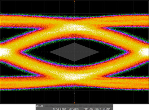
Image: The eye diagram shows the excellent results and wide margin of the Synopsys DesignWare USB 3.0 femtoPHY silicon in 14-nm FinFET process technology.
Synopsys developed the USB 3.0 and USB 2.0 femtoPHY IP to enable designers to select the optimal implementation for their application without sacrificing the features or capabilities required for USB compliance certification. Designs requiring high performance can take advantage of the USB 3.0 femtoPHY's 5.0 Gbps data transfer rates per the SuperSpeed USB (USB 3.0) specification. Applications requiring lower performance can implement the USB 2.0 femtoPHY's 480 MHz data transfer rates per the Hi-Speed USB (USB 2.0) specification. Both DesignWare USB femtoPHYs minimize the number of pins needed on the SoC periphery to further reduce SoC area and cost. Power down features minimize battery drain when the PHY is inactive, while retaining all PHY states to enable fast, accurate power-on capabilities. In addition, the DesignWare USB femtoPHYs support the popular USB Battery Charging v1.2 specification and the USB On-The-Go (OTG) v2.0 protocol.
"As an active member of the USB-IF for more than 18 years, Synopsys continues to develop IP products that ease the integration and adoption of the USB 3.0 and USB 2.0 interfaces," said Jeff Ravencraft, president and COO of the USB Implementers Forum. "USB-IF certification demonstrates that a product meets USB-IF interoperability standards and is compliant with the corresponding USB specification. The availability of Synopsys' new, smaller area DesignWare USB 3.0 and USB 2.0 femtoPHYs gives manufacturers the ability to incorporate this technology into their SoCs."
"SoC designers have relied on Synopsys for USB interfaces in more than 3,000 designs and more than 100 process technologies, making us the leading USB IP provider for more than a decade," said John Koeter, vice president of marketing for IP and prototyping at Synopsys. "Our technical expertise and track record in delivering high-quality IP for advanced process technologies enables designers to integrate IP that reliably meets their stringent application requirements. With the availability of DesignWare USB 3.0 and USB 2.0 femtoPHY IP, backed by FinFET silicon success, we can help our customers meet the industry demand for smaller, cost-effective, high-performance SoCs."
Availability
The DesignWare USB 2.0 and USB 3.0 femtoPHY IP are available now in leading 14/16-nm FinFET and 28-nm process nodes.
About DesignWare IP
Synopsys is a leading provider of high-quality, silicon-proven IP solutions for SoC designs. The broad DesignWare IP portfolio includes complete interface IP solutions consisting of controllers, PHY and next-generation verification IP for widely used protocols, analog IP, embedded memories, logic libraries, processor solutions and subsystems. To support software development and hardware/software integration of the IP, Synopsys offers drivers, transaction-level models, and prototypes for many of its IP products. Synopsys' HAPS® FPGA-Based Prototyping Solution enables validation of the IP and the SoC in the system context. Synopsys' Virtualizer™ virtual prototyping tool set allows developers to start the development of software for the IP or the entire SoC significantly earlier compared to traditional methods. With a robust IP development methodology, extensive investment in quality, IP prototyping, software development and comprehensive technical support, Synopsys enables designers to accelerate time-to-market and reduce integration risk. For more information on DesignWare IP, visit http://www.synopsys.com/designware.
About Synopsys
Synopsys, Inc. (Nasdaq:SNPS) accelerates innovation in the global electronics market. As a leader in electronic design automation (EDA) and semiconductor IP, Synopsys delivers software, IP and services to help engineers address their design, verification, system and manufacturing challenges. Since 1986, engineers around the world have been using Synopsys technology to design and create billions of chips and systems. Learn more at www.synopsys.com. |
|
|
|
|
|